
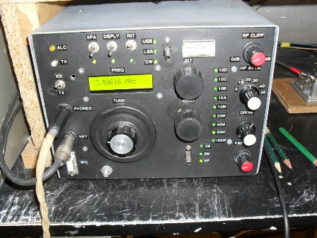
Described here is a transceiver covering HF ( no warc bands ), 6m and 2m. Modes of operation are USB, LSB and CW. Power output on HF is 10W, 6m 5W and 3W
on 2m. Linear amplifiers are used to bring the power up to legal limit. Tx audio produced is very good as is CW note. HF rx is subjectively better than a Trio
TS530 ( I had one in for repair that was used as a comparison ). The 10m band is used as a tuneable IF for 6 and 2m, effectively a transverter. 2m performance is comparable to a FT480. This is not a full
construction article as much of it will be up to the individual, however all of the important aspects are covered.
Circuit diagrams are given for the main board and the 2m transverter section, if time allows i will include a circuit for the 6m transverter.
No documentation was kept for the local oscillator chain hence a brief descrition is given. The set has been in use for five years now and has given excellent service.
The set is a single conversion superhet using an IF frequency of 9MHz ( similar to the FT200 ) as cheap comercial CW and SSB crystal filters are commonly available at this frequency.
A digital frequency readout using a pic and LCD display is used to give an accurate frequency indication on all bands. Surface mount components have mainly been used in the
construction of the PCB's to reduce size.
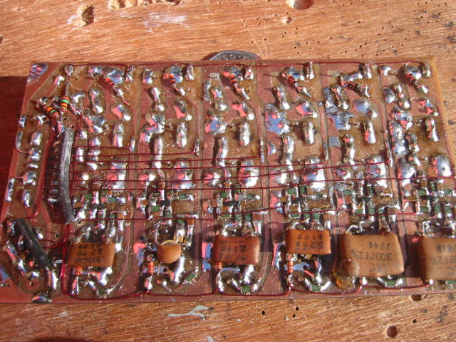

The front end of the transceiver consists of a bandbpass filter for each HF band followed by a Mosfet preamp stage.
Mosfets were chosen for there good strong signal handling. Each filter stage is selected by DC wetted relays, pin diodes were avoided in this
early stage to preserve intermod performace. As the relays are DC wetted long contact life is ensured. The same result could be acheived with a single
Mosfet and a complex bandswitch for the various bands, however a complex and potentialy troublesome bandswitch was avoided and Mosfets are reasonably cheap.
The bandpass filter is used for both receive and transmit, a set of DC wetted relays is
used to acheive this. Agc and power output control is acheived by varying the Mosfet G2 voltage. The source of the Mosfet is jacked up at roughly 3 volts ( depending on the drain current )
this allows a much greater agc range as the G1 can effectively be taken down to minus 3 volts with respect to the source. All coils were wound on old CB type IF transformers, winding
details are given in the circuit diagram
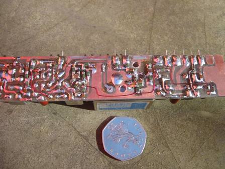
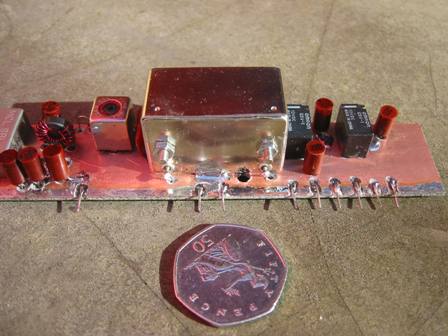
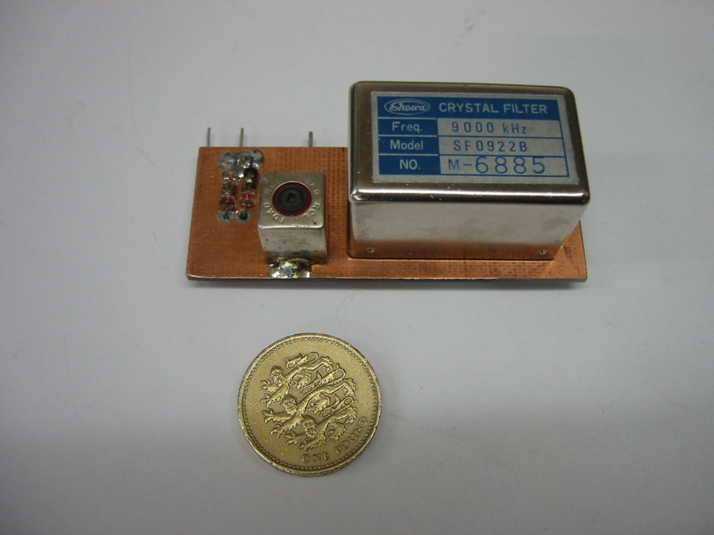
In receive mode the output from the input bandpass module is fed to the SBL-1 double balanced mixer located on the mixer / SSB filter board. The IF output from the mixer is then passed through the SSB crystal filter via the grouned gate jfet amplifier. Correct mixer termination is provided by the T - pad attenuators on the LO and IF ports of the SBL-1. The signal is then also passed through the CW crystal filter ( which is mounted on a seperate small board due to lack of space ) if CW is selected. The dual gate mosfet ahead of the CW filter makes up for the inserstion loss of the CW filter which is somewhat higher than the SSB filter. From here the signal is then fed to the IF module. Circuit diagram
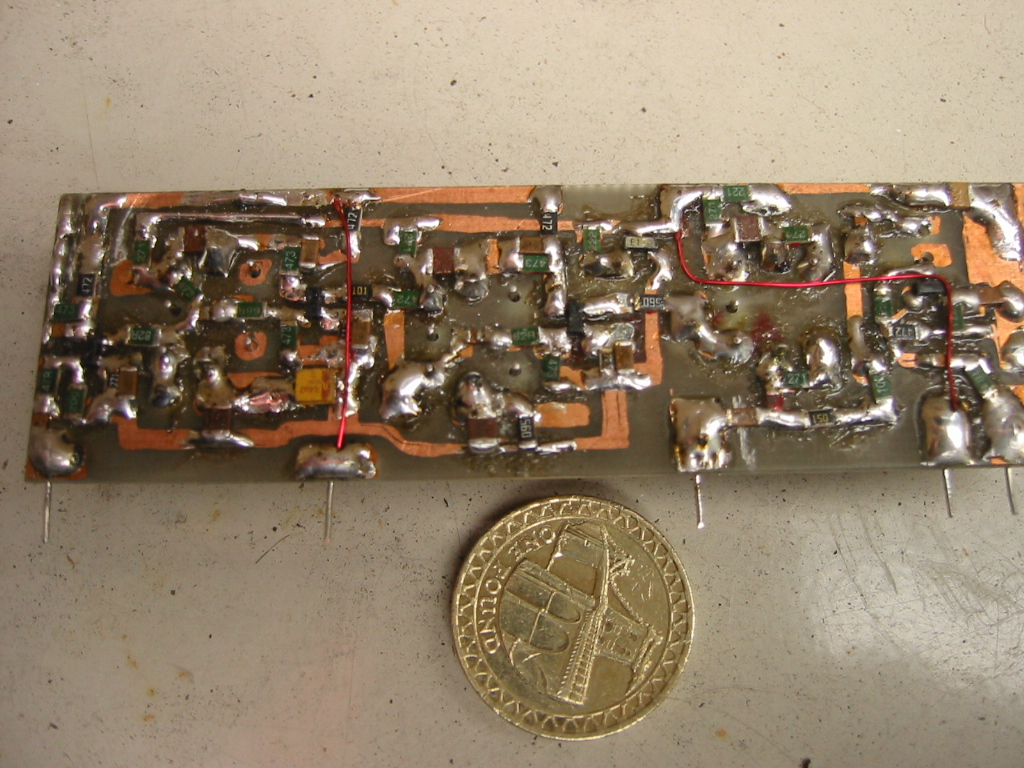
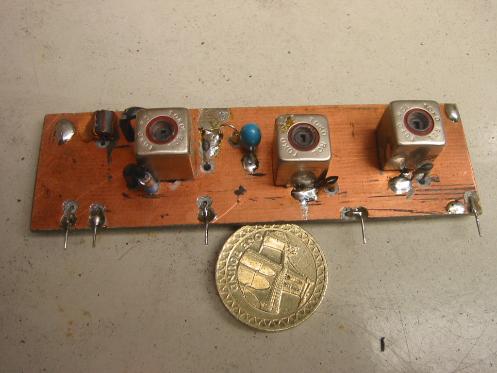
The IF amplifier consists of three cascaded dualgate Mosfets. This arrangement was chosen for its excellent agc range and performance. Again, the sources of the Mosfets are jacked up
at 3 volts for improved agc range. A diode product detector is used for demodulation consisting of a couple of OA91's. Here is the circuit diagram for the IF amplifier
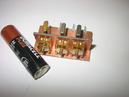
Three seperate CIO's are used to feed the product detector for demodulation. LSB and USB CIO's are also used for DSB generation when SSB Tx is selected. A seperate oscillator is used for CW Tx carrier generation,
here are the circuit diagrams

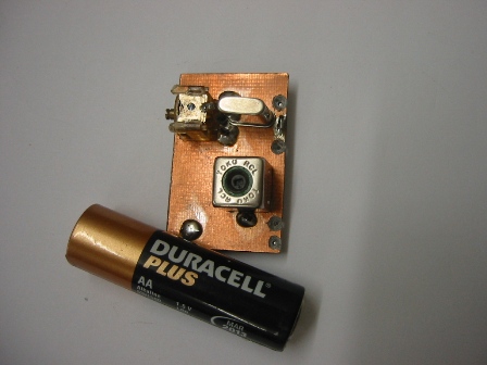
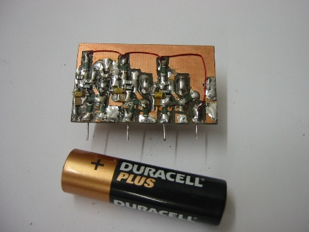
Bottom left hand side is a photo of the CW carrier oscillator module
IF derived AGC is used for its good attack characteristics due to the small time constants involved at 9MHz. The IF signal from the drain of the last Mosfet in the IF amplifier is fed into a Jfet
tuned amplifier. The signal is further amplified by a low gain untuned bipolar stage. From here the signal is fed into a charge pump circuit consisting of two diodes and a R/C time constant network
( a 1k and 100nF ). The DC voltage produced by the charge pump circuit is amplified by a two transistor DC amplifier, AGC control voltage is taken from the emitter of the last transistor and a S - Meter
voltge from it's collector. The AGC system gives very good performance for a simple circuit
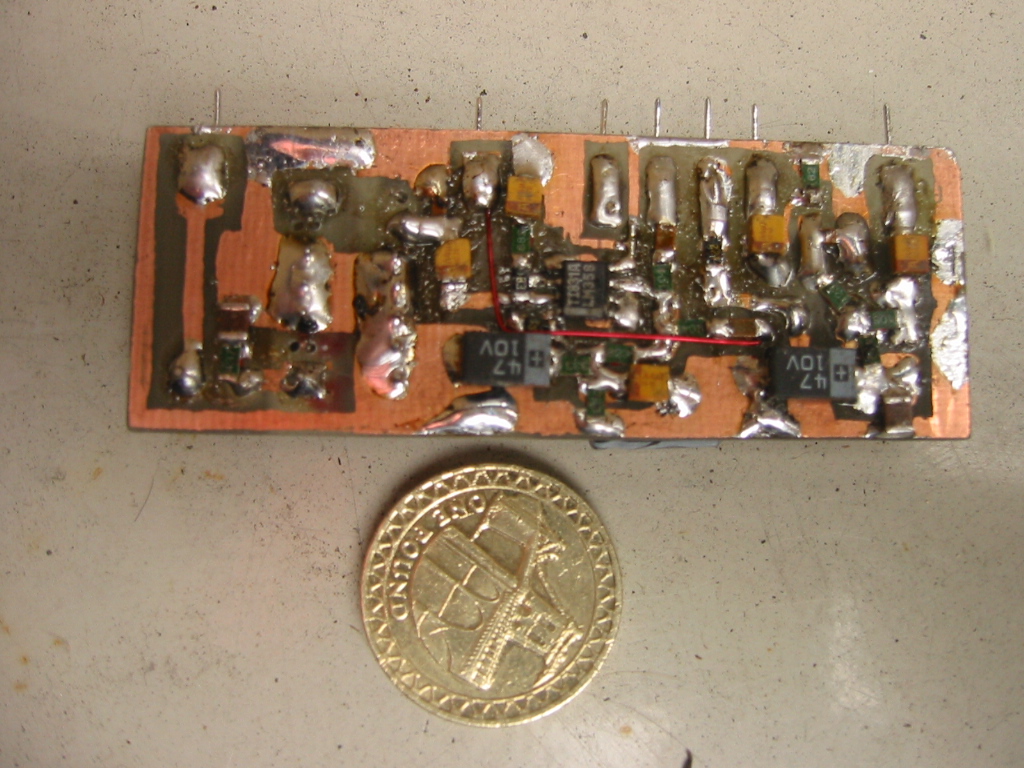
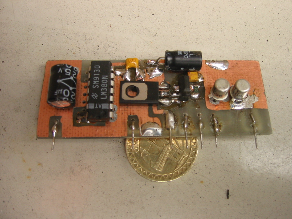
The receive AF amplifier module is very straight forward, looking at the circuit diagram you will see the demodulated audio signal is fed to a one transistor preamp
and then to a emitter follower buffer. Top cut is applied between these two stages by a simple R/C network ( 12k and 10nF ). The received audio and CW sidetone is mixed by a op amp the output of which
is fed to the audio PA ( LM380 )
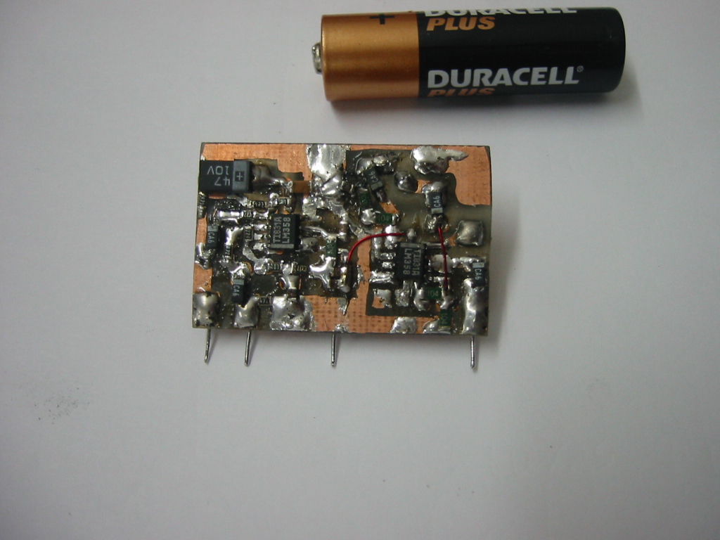
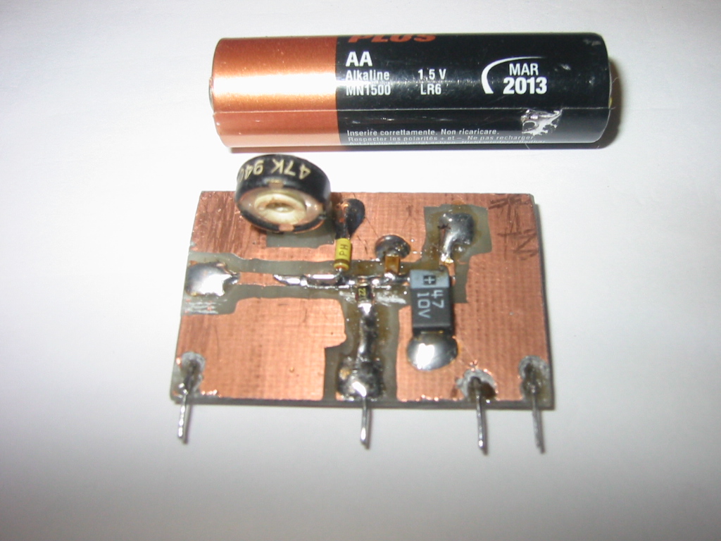
A balanced audio input mic preamp is used here as i wanted to be able to run a long mic cable to the set if needed. Ic1a provides a small amount of gain and also convrts the balanced audio into
unbalanced audio. HF roll off is provided by a top cut filter ( a low pass filter ) consisting of Ic1b, the turnover frequency is approximately 2.5KHz. Ic2a
provides more gain and determines the LF roll off which is roughly 300Hz. From here the audio is passed through a Mic level preset and then on to a op amp buffer stage where it is then fed to
the DSB generator. circuit diagram.
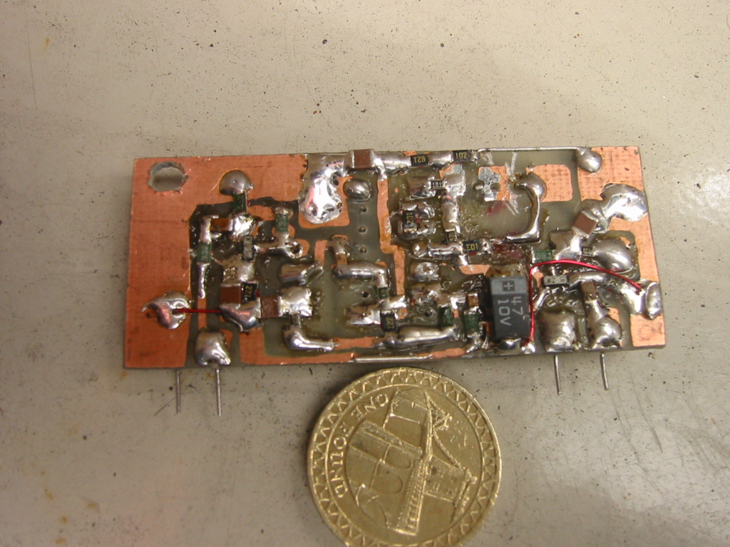
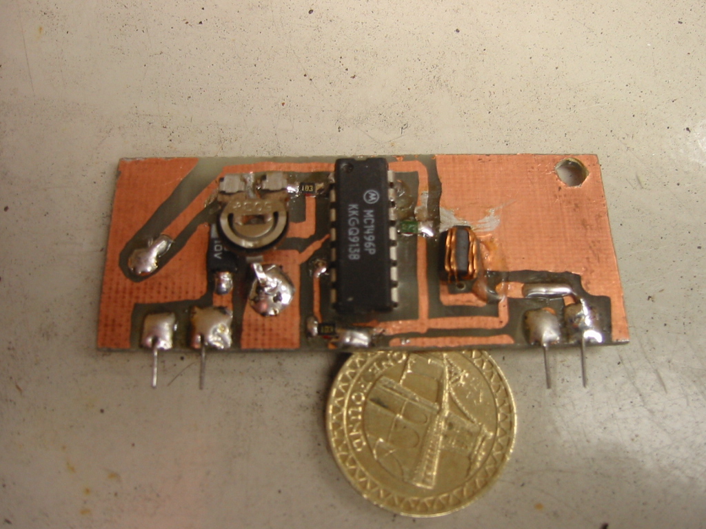
USB or LSB carriers are fed into a single transistor gain stage who's output is fed into pin 8 of the MC1496p, the resistor in series with the transistors base is adjusted to produce 180mVpp on pin 8 of the chip. Audio from the mic preamp module is also fed into 1 of the chip. The MC1496p is configured as a balanced modulator, double sideband suppressed carrier appearing on pins 6 and 9. A NE602 would also be suitable for this application, however I have lots of MC1496p's in the junk box. A transistor buffer stage is used for impedance matching/isolation to the next stage ( RF speech clipper module ). CW Tx carrier and clipped SSB enter the SSB/CW filter module via Tr3 ( depending on whether SSB or CW is selected ) on the filter board. Tr3's collector load of a 560R resistor provides correct termination for the SSB crystal filter. Clipped SSB and CW Tx carrier exit the filter via Tr2 and D2 where they are than fed to the SBL-1 double balanced mixer. Here the 9MHZ SSB or CW signal is mixed with the local oscillator signal to produce the required band ( plus other unwanted frequencies ). The output from the mixer is then fed to the input bandpass filter module. Here the bandpass filter selects only the wanted signal, also, power control is also applied by altering the Mosfet G2 voltage. From the output of the bandpass filter module the low level RF signal is then routed to the HF driver and PA or to the 6m and 2m transvertors via DC wetted relays. The routing and logic circuitry is not shown here, I will leave that up to the indivdual.DSB generator circuit diagram.
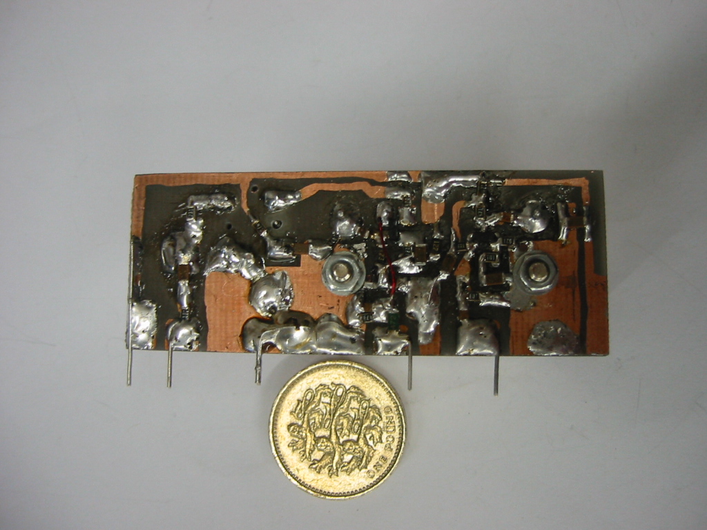
Although CW is my primary mode of operation, i did feel an RF speech clipper would be useful for phone work despite the extra cost of another SSB crystal filter to acheive this. DSB is fed into a transistor amplifier, the 560R collector load once again providing correct termination for the SSB crystal filter. SSB leaves the filter where it is amplified by a gain controlled dual gate Mosfet with a tuned drain load. The secondary of the drain load is coupled to a diode RF clipper. Thus the amount of clipping produced is varied by the gain of the Mosfet which in turn is controlled by its G2 voltage. The clipped SSB is then fed to another SSB crystal filter located on the SSB/CW filter module, here the HF distortion products are greatly attenuated. In use the speech clipper has proved very effective and not as nasty sounding as audio clippers, this is due to the excellent filtering provided by the second SSB filter ( albeit, there will still be some inband distrtion products but the net result is very good ). Approximately 20dB of clipping can be produced with this circuit
The HF driver consists of a two transistor broadband amplifier identical to the one used in the 80m/20m HF set shown elsewhere on this site. The final PA uses two RDH16FF1's in a broadband push pull configuration, power output is approximately 10 watts. This is followed by the usual switched low pass filter arrangement.
The local oscillator consists of a free running VFO ( 5MHz - 5.5MHz as used in the 80m/20m HF set but with the final transistor stage omitted ) which is mixed with the relevent band crystal, a seperate band oscillator and crystal is used for each HF band. A NE602A is used as a double balanced mixer to mix the two frequencies. This is followed by a passive two pole bandpass filter ( as used in the input bandpass filter module but with no Mosfets ) and finaly a two stage broadband amplifier ( same as HF driver ), the output of the amplifier is padded down to a suitable level for driving the SBL-1 double balanced mixer and the pic frequency display ( same as 80m/20m HF set ). As an exaple for 10m the band crystal = Fo minimum ( 28.00 MHz ) + IF ( 9MHz ) - VFO minimum ( 5.0 MHz ) = 32MHz. No crystal is required for 20m as the VFO is used direct as LO.
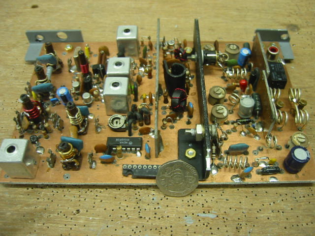

The 2m transverter is fairly conventional, a 38.666MHz crystal oscillator is frequency multiplied by 3 to give a LO injection of 116MHz for the RX and Tx mixers. A dual gate mosfet rf stage is utilised followed by a dual gate mosfet mixer for the Rx side of the
transverter. For transmit, a MC1496p is used as a balanced mixer follwed by a two pole 2m band pass filter and a dualgate mosfet which is used for Tx power control, see circuit diagram. The 2m PA chain is also conventional, a two transistor broad band
class A stage preceeds a two transistor 2m tuned linear PA.
Barry Zarucki M0DGQ
HOME